If You Need World PCBA For Your Bussiness, Please Contact Us!


Type of PCB:
Number of layers:
Overall dimensions of PCB:
Final boards thickness:
Copper weight:
Surface finishing:
Plugging or Filling holes:
Soldermask:
Special technology:
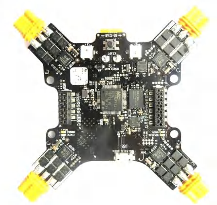
Application:
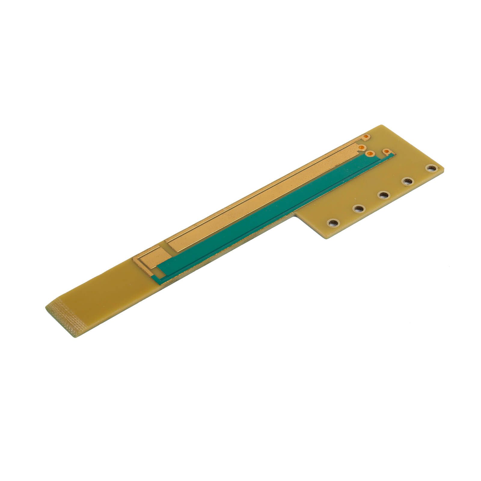
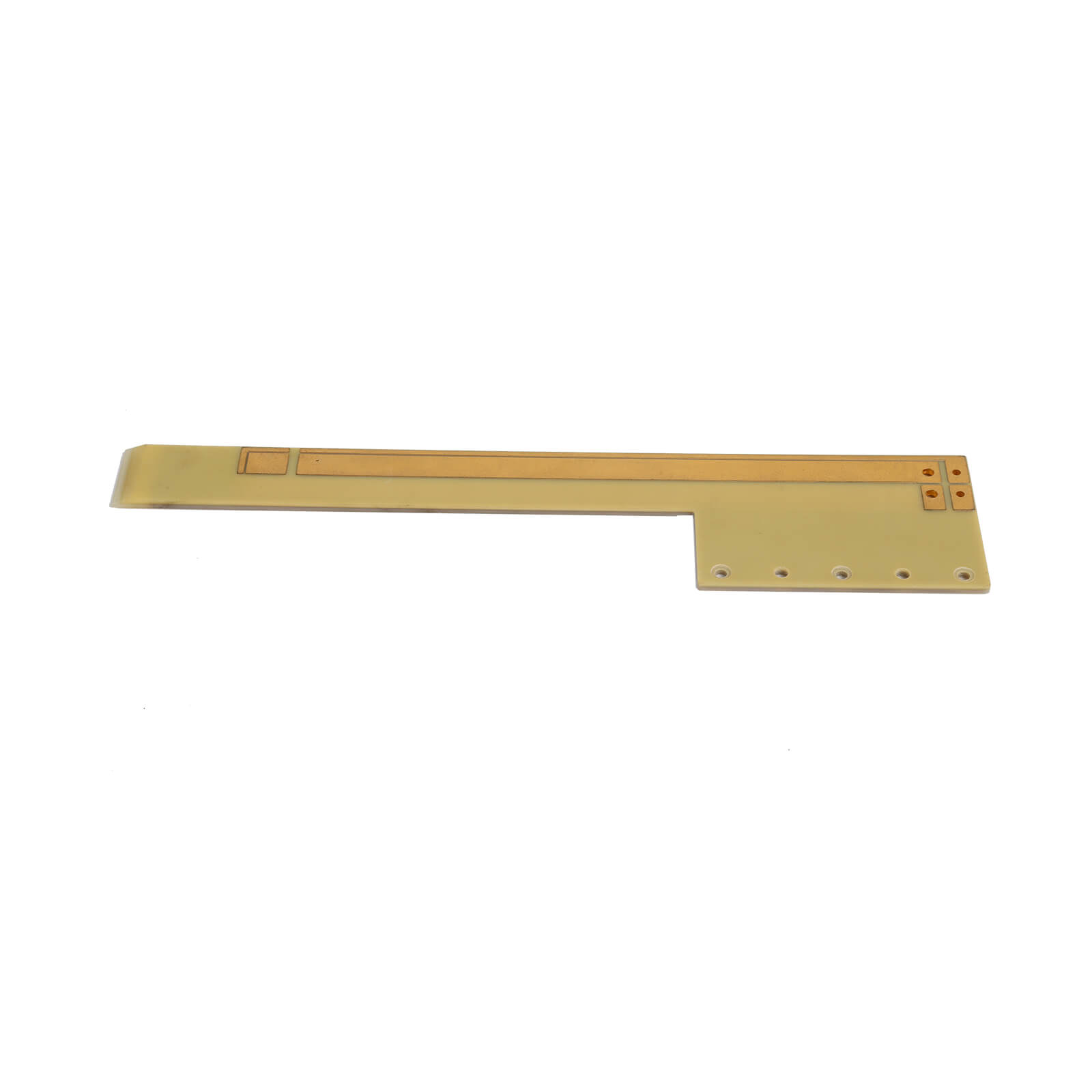
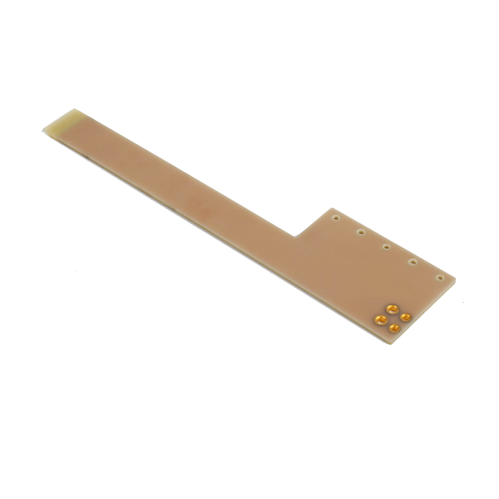
2layer Depth Control Drilling PCB | |
Name: | 2Layer Depth Control Drilling PCB |
Material: | TG180 FR4 |
Thickness: | 1.60mm |
Layer: | 2L |
Copper: | 35um |
Soldermask: | NO |
Surface finished: | Immersion gold |
Min.Line width | 75um |
Min.Line spacing: | 75um |
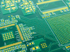
H-CELERITY PCB LIMITED Medium and small batch multi-layer PCB board manufacturing, 4-32 layer PCB processing technology, minimum line width/spacing 2.5/2.5mil, copper thickness up to 12oz, meet the high heat dissipation requirements of power products,support blind hole, nickel palladium, selective gold, step hole groove, inner and outer layer impedance matching, resistance range: 45-110Ω.
Multilayer PCB boards production capacity:
1 | Layer | 1-32layer | |
3 | Raw Material | FR-4 | |
4 | Soldermask | Taiyo,Guangxin | |
5 | Max size | 1000×600mm | 4layer:1000*500mm |
6layer:900*500mm | |||
8layer:625*500mm | |||
10/12layer:400*300mm | |||
6 | Min size | 1×1mm | |
7 | Max boards thickness | 6.0mm | Standard:0.10/0.15/0.25/0.3/0.4/0.6/0.8/1.0/1.2/1.6/2.0/2.4/3.0mm |
8 | Min boards thickness | 0.10mm | |
9 | Min core thickness | 0.04mm | 40um |
10 | boards tolerance | ±10% | Min. 0.03mm |
12 | bow and twist | 0.75% | special controlled ≤0.5% |
13 | Max drilling | Φ6.5mm | Special > 6.5mm |
14 | Min drilling | Φ0.05mm | Standard: > 0.15mm |
17 | Min copper thickness | 1/8oz | standard: 1/2oz |
18 | Max copper thickness | 12oz | standard: 2-6oz |
23 | PTH tolerance | ±0.075mm | Special: ±0.05 |
24 | NPTH tolerance | ±0.05mm | |
25 | Hole shift tolerance | ±0.05mm | |
26 | Vias copper | ≥20μm | |
27 | Outlayer design rule(Line width/spacing) | T/Toz: 2.5mil/2.5mil(T=1/3oz) | |
H/Hoz: 2.5mil/2.5mil | |||
1/1oz: 3mil/3mil | |||
2/2oz: 6mil/6mil | |||
3/3oz: 10mil/10mil | |||
4/4oz:14 mil/14mil | |||
28 | Inner layer design rule (Line width/spacing) | T/Toz: 2.5mil/2.5mil(T=1/3oz) | |
H/Hoz: 2.5mil/2.5mil | |||
1/1oz: 3mil/3mil | |||
2/2oz: 6mil/6mil | |||
3/3oz: 10mil/10mil | |||
4/4oz:14 mil/14mil | |||
29 | Etching tolerance | ±20% | Special: 10% |
34 | Min soldermask bridge | 2mil | |
35 | Soldermask filled vias | ≤0.45mm | |
36 | electroless nickel immersion gold/nickel | 100-200uin(μ") | |
37 | ENEPIG standard | NI:200u" | |
Pd:1-10u" | |||
Au:1-10u" | |||
38 | electroless nickel immersion gold/gole | 1-3uin(μ") | special: 5-200U" |
39 | Tin thickness(HASL) | 2-40μm | |
40 | Selective Electric gold + Gold finger | AU:3-100u" | no plated line residual |
42 | Routing tolerance | ±5.2mil(0.13MM) | Larser ±2mil(0.05MM) |
43 | Hole to edge tolerance | ±7mil(0.177MM) | Special ±6mil(0.15MM) |
44 | Min inside Angle | R≥0.5mm |
Email us, we will send the multilayer PCB stack up PDF file to you for design reference.
We will contact you as soon as possible!
FR-4 2Layer Depth Control Drilling
Specialized in PCB & PCBA manufacture in CHIAN

Enter your email and we will contact you within 24 hours
 English