PCB Boards

If You Need World PCBA For Your Bussiness, Please Contact Us!

Ceramic board

Product Description

Ceramic Printed Circuit Boards (PCBs) by H-CELERITY PCB LIMITED

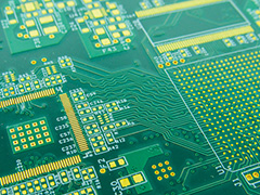
H-CELERITY PCB LIMITED specializes in the manufacture of high-quality Ceramic Printed Circuit Boards (PCBs), which are designed to meet the stringent demands of industries requiring exceptional thermal conductivity, electrical insulation, and mechanical stability. Our ceramic PCBs are engineered using state-of-the-art process technologies and materials to deliver unparalleled performance and reliability.

Key Technologies

  • Direct Bond Copper (DBC): This technology involves bonding a thin layer of copper directly onto a ceramic substrate using a high-temperature process. DBC is ideal for applications requiring high thermal conductivity and excellent electrical insulation, making it perfect for power electronics and high-power LED applications.

  • Direct Plated Copper (DPC): Utilizing photolithographic techniques, DPC allows for the precise deposition of copper layers on the ceramic substrate, enabling fine-line circuits and high-frequency performance. This technology is particularly useful in RF and microwave applications.

  • Active Metal Brazing (AMB): AMB utilizes brazing alloys to join copper to the ceramic substrate, allowing for the creation of complex structures and high-temperature applications. This technology is often used in aerospace and defense sectors.

  • High-Temperature Co-fired Ceramics (HTCC): HTCC involves printing conductive pastes (containing metals like tungsten or molybdenum) onto a green (unfired) ceramic tape, which is then co-fired at high temperatures. This results in a dense, reliable structure suitable for high-temperature environments.


Ceramic PCB

Common Materials

  • Aluminum Oxide (Al₂O₃): Known for its good dielectric strength and thermal shock resistance, Al₂O₃ is a popular choice for general-purpose ceramic PCBs.

Al2O3

  • Aluminum Nitride (AlN): With higher thermal conductivity than Al₂O₃, AlN is often used in applications requiring better heat management, such as high-power electronics and LED lighting.

Leading Manufacturers
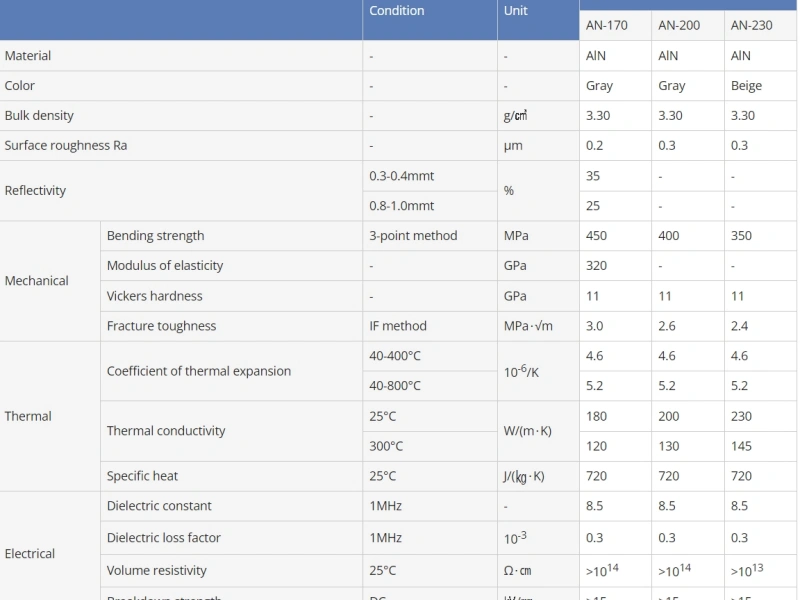
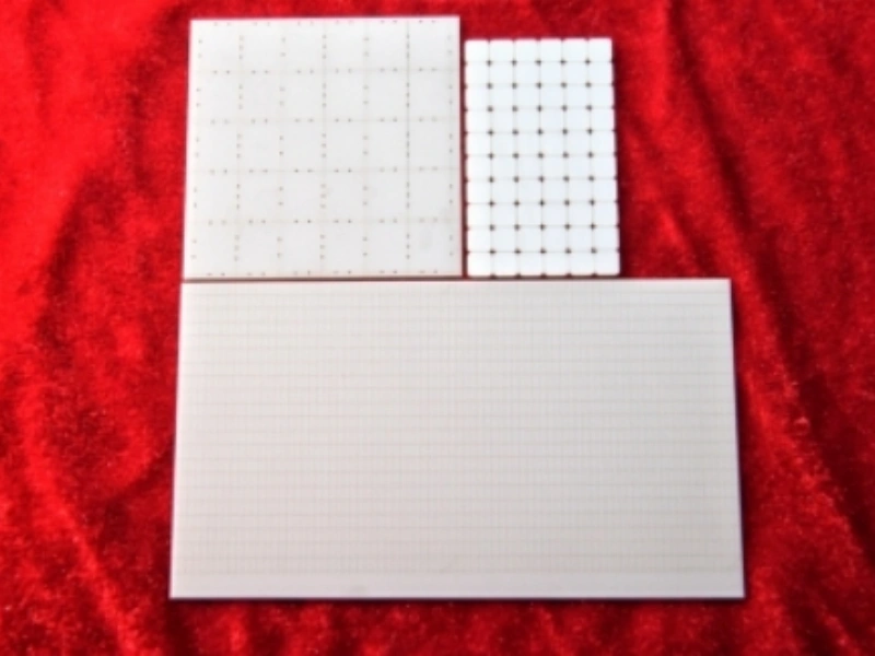
  • Maruwa: A well-established manufacturer known for their advanced ceramic materials and components.


General Dimension


ItemUnitType
AN-170AN-200AN-230
Dimensioninch(max)5.5"×7.5"5.5"×7.5"5.0"×7.0"
Tolerance±1% NLT:±0.1㎜±1% NLT:±0.1㎜±1% NLT:±0.1㎜
Thickness0.25~1.50.25~1.50.25~1.0
Tolerance±10% NLT:±0.04㎜±10% NLT:±0.04㎜±10% NLT:±0.04㎜
Through holeΦ0.2~Φ0.2~Φ0.2~
Tolerance±0.05㎜±0.05㎜±0.05㎜
Warpage0.002/㎜0.002/㎜0.002/㎜


  • Huaqing: A reputable supplier offering a wide range of ceramic PCB solutions tailored to specific customer needs.

Contact Us

If you have any requirements for ceramic PCBs, whether it's for prototyping or mass production, H-CELERITY PCB LIMITED is here to help. Our team of experts will work closely with you to ensure that your custom ceramic PCB meets all your specifications and exceeds your expectations.

For more information or to request a quote, please contact us at sales@h-cpcb.com.


Ceramic Board Materials Classification

Ceramic PCBs utilize different materials to suit specific application requirements. The most commonly used materials include:

  • Aluminum Oxide (Al₂O₃): Known for its good dielectric strength and thermal shock resistance, Al₂O₃ is a popular choice for general-purpose ceramic PCBs.

  • Aluminum Nitride (AlN): With higher thermal conductivity than Al₂O₃, AlN is often used in applications requiring better heat management, such as high-power electronics and LED lighting.

Ceramic Board Production Manufacturing Capabilities

At H-CELERITY PCB LIMITED, we have the capacity to produce ceramic PCBs in both small quantities for prototyping and large volumes for mass production. Our state-of-the-art manufacturing facility is equipped with the latest machinery and tools to ensure consistent quality and precision.

ItemThick Film Ceramic BoardDBC/DCB Ceramic PCBDPC  Ceramic PCBAMB Ceramic PCB
Layer6 Layer2 Layer2 Layer2 Layer
Max size200*200mm138*178mm138*190mm114*114mm
Min thickness0.15mm0.30mm~0.40mm0.15mm0.25mm
Max thickness6.0mm1L: 1.3mm; 2L: 1.6mm6.0mm1.8mm
conductor thickness5um-40um3.9oz-8.6oz2um-200um8oz-22.9oz
Min line width/sapcing6mil/6mil(0.15/0.15mm)12/12mil (0.30/0.30mm)3/3mil (0.075/0.075mm)20/20mil (0.50/0.50mm)
MaterialAl2O3,AlN, BeOAl2O3,AlN,ZrO₂Al2O3,AlNAlN,Si₃N₄,ZrO₂

ZrO₂,Si₃N₄
Material thickness0.25, 0.38, 0.50, 0.635,0.80,1.0, 1.25, 1.5, 2.0mm0.25, 0.38, 0.500.25, 0.38, 0.50, 0.635,    0.80,1.0, 1.25, 1.5, 2.0mm0.25, 0.38, 0.50,


0.635,0.76, 1.0mm0.635, 0.76,1.0mm
Min holes4mil (0.1mm)
Min PAD ring6mil(0.15mm)N/A3mil (0.075mm)N/A
Min PTH in wall3milN/A4mil (10um)N/A
Min pad size10mil (0.25mm)8mil (0.20mm)6mil (0.15mm)8mil (0.20mm)
Min soldermask bridge12mil (0.30mm)8mil (0.20mm)6mil (0.15mm)8mil (0.20mm)
Min BGA ball gap12mil (0.30mm)8mil (0.20mm)5mil (0.125mm)8mil (0.20mm)
PTH/NPTH tolerencePTH: ±4mil (0.1mm) ; NPTH: ±2mil (0.05mm)
hole offset toleranceL/D± 0.1mm/Thk± 0.05mm
outline toleranceLaser: +0.2/0.05mm;Laser: +0.2/0.05mmLaser: +0.2/0.05mm;Laser: +0.2/0.05mm


Punching: +0.25/0.20mmPunching: +0.25/0.20mm
Line width/spacing tolerence± 5mil (0.125mm)± 5mil (0.125mm)± 1mil (0.025mm)± 5mil (0.125mm)
Surface finishedAgPd,AgPt,AuOSP,Nickel plated, Immersion goldOSP,ENIG,NiPdAuOSP,Ni plated,ENIG
thermal stress1 hour @ 350℃3 x 10 Sec @ 280 ℃15 min @ 350 ℃3 x 10 Sec @ 280 ℃

Our production capabilities include:

  • Advanced Material Handling: Precise handling of ceramic substrates to minimize defects during the manufacturing process.

  • Fine-Line Circuitry: Capable of producing fine-line circuits for high-density interconnect applications.

  • Custom Design Services: Our design team works closely with clients to develop custom solutions tailored to specific requirements.

Ceramic Board Applications

Ceramic PCBs find applications in a wide range of industries, including:

  • Power Electronics: High-power converters, inverters, and power modules.

  • Aerospace & Defense: Radar systems, satellite communication devices, and avionics.

  • Automotive Industry: Electric vehicle power electronics, battery management systems, and sensor technologies.

  • Medical Equipment: Imaging devices, diagnostic equipment, and surgical tools.

  • Telecommunications: RF and microwave components, antennas, and signal processing boards.

Ceramic Board Product Showcase

We offer a comprehensive range of ceramic PCB products, each tailored to meet the unique needs of our clients. Our product lineup includes:

  • Standard Ceramic PCBs: Suited for general applications requiring basic thermal and electrical properties.

  • High-Frequency Ceramic PCBs: Optimized for applications requiring low loss and high-speed signal transmission.

  • High-Power Ceramic PCBs: Designed for applications with high current densities and demanding thermal management requirements.

Contact Us

For all your ceramic PCB needs, H-CELERITY PCB LIMITED is here to help. Our team of experts will work closely with you to ensure that your custom ceramic PCB meets all your specifications and exceeds your expectations.

To learn more about our ceramic PCB solutions or to request a quote, please contact us at sales@h-cpcb.com


Tags:

Got Free Inquiry Now

We will contact you as soon as possible!

Subject

Ceramic board

If you have questions or suggestion,please leave us a message,we will reply you ad soon as we can!

H-CELERITY PCB LIMITED

Specialized in PCB & PCBA manufacture in CHIAN

+86-15816888615
+86-0755-36931652
sales@h-cpcb.com
#A5-A7 Building, Xinbaoye Industrial Park, #2ND Daxing,Shajing Town, Baoan District, Shenzhen-518124.
Copyright © 2023 H-CELERITY PCB LIMITED Co., Ltd. All Rights Reserved.   Privacy Policy   Powered by Bontop